Saturday, December 31, 2011
BJT output current protection


Friday, December 30, 2011
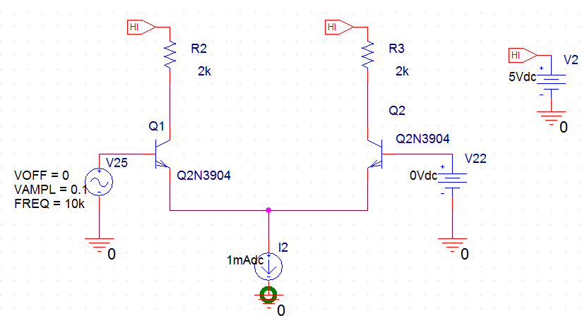
BJT active load


Vout = Vc(Q4) = Vc(Q3) ~ V(R10) ~ V(R9 or R11) = I(R9)*R9 ~ (Ic(Q8)/2)*R9.
Current output from wilder current source varies little => Vout varies little.


Ib(Q3) + Ib(Q4) + Ic(Q3) + Ic(Q4) ~ IC(Q8). If Ic increase, Ib will decrease, which in turn result in Ic decrease. The feedback loop of the active load keep system stable.


also the current source becomes unstable.
Thursday, December 29, 2011
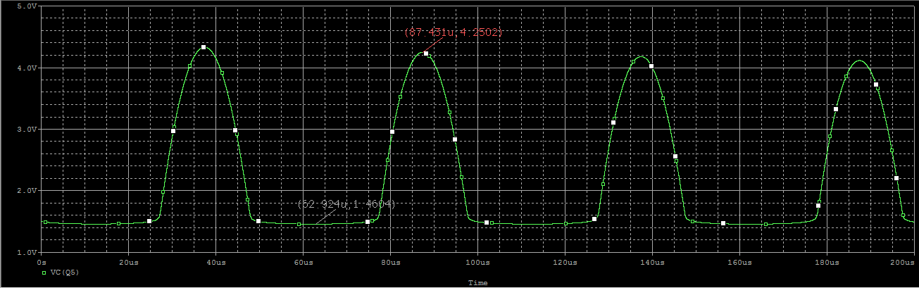
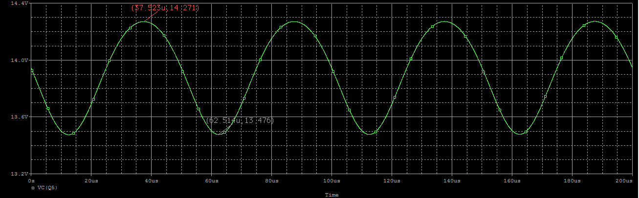
multi-stage differential pair


stage2: second differential pair outputs 50mv peak deviation sin signal( 16.7 times amplification).

stage3:transistor 5 outputs 900mv peak deviation sin signal( 18 times amplification),
transistor 5 acts as a level shifter as well, design the collector and emitter resistors so that dc voltage at emitter of transistor 5 is 0.7v. (so that output dc voltage at emittor of transistor 6 is 0v).

transistor 6 acts as a buffer. It has a low output inpedance.
Total gain = 900mv/0.1mv = 9000!
Wednesday, December 28, 2011
differential pair

Works well for amplifying small signal(under 100mv)


peak output difference 12.5v( 125 times amplification!).

By adding resistor at the emitter, we have more control of the gain.
AC gain = 2*Rc/[2*(RE + Re)] = Rc/(RE + Re). (RE is within hybrid pi model of transistor, Re is the resistor we just added). In this case Re >> RE, gain ~ Rc/Re = 50.

We need to adjust VCC, current source, and Rc to keep transistor in operation mode.
Tuesday, December 27, 2011
BJT


Gain = 4.5409/0.0193 = 235.279. (from simulation).
Gain = -gm*(r0||Rc) ~ -gm*Rc. (formula) (r0 resistor within hybrid pi model of transistor, usually large).
gm = Ic/VT = 662uA/26mv = 0.025461.
Gain = 254.6 (from formula) close to simulation.
Note: R3/R5 = R4/R6 to keep transistor in operation mode.

change R5 to 20K, transistor in saturation mode. (collector voltage = VCC).
Collector output binded.

Monday, December 26, 2011


Sunday, December 25, 2011
Instrumentation amplifier

Nodal analysis
Vz = R3/(R2 + R3)*Vy;
(Vz - Vx)/R2 = (Vout - Vz)/R3;
Vout = (R3/R2)*(Vz - Vx) + Vz = (R3 + R2)/R2*Vz - R3/R2*Vx = R3/R2*(Vy - Vx);
Vy - Vx = -(V1 - V2)*(Rgain + 2*R1)/Rgain;
Vout = -(V1 - V2)*[(Rgain + 2*R1)/Rgain]*(R3/R2);
high pass, low pass filter

2nd order high pass


1st order high pass


1st order low pass


2nd order low pass

Vout/Vin = [1/(RC)^2]/[S^2 + 2/(RC)*s + 1/(RC)^2]

W0 = 1/(RC); Q = 1/2;
Critical damped system: the steepest decay slope without overshoot.
Subscribe to:
Comments (Atom)